Research Abstract
成型可能な全カーボン集積回路
Mouldable all-carbon integrated circuits
2013年8月6日 Nature Communications 4 : 2302 doi: 10.1038/ncomms3302
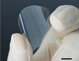
日用品から電気製品や医療機器に及ぶさまざまなプラスティック製品は、成型技術によって作られている。しかし、さまざまなプラスティック製品に電子回路を組み込むことは、シリコンウェハーのもろい性質によって制限されている。今回我々は、成型できる集積回路を初めて報告する。このデバイスは、全てがカーボン系材料でできている。つまり、このデバイスの能動チャネルと受動素子は全て、伸縮可能で熱的に安定なカーボンナノチューブの集合体とプラスティックポリマーの誘電体層や基板から作られている。この全カーボン薄膜トランジスターは、移動度1,027 cm2V−1s−1とオンオフ比105を示す。さらに、このデバイスは、熱圧成型したときに、最大18%という極めて優れた2軸伸縮性も示す。我々は、機能する集積回路を三次元的なドームに成型できることを実証している。このような成型可能な電子機器によって、プラスティック製品に電子的機能を、電気製品にプラスティックのような機能を加えることができるため、新たな可能性が開かれ、デザイン性を向上できる。
Dong-Ming Sun1*, Marina Y. Timmermans2, Antti Kaskela2, Albert G. Nasibulin2, 岸本 茂1, 水谷 孝1, Esko I. Kauppinen2 & 大野 雄高1, 3
- 名古屋大学 量子工学専攻
- アールト大学(フィンランド)NanoMaterials Group, Department of Applied Physics and Center for New Materials
- アールト大学(フィンランド)Multidisciplinary Institute of Digitalisation and Energy
*現所属先:中国科学院(中国)
A variety of plastic products, ranging from those for daily necessities to electronics products and medical devices, are produced by moulding techniques. The incorporation of electronic circuits into various plastic products is limited by the brittle nature of silicon wafers. Here we report mouldable integrated circuits for the first time. The devices are composed entirely of carbon-based materials, that is, their active channels and passive elements are all fabricated from stretchable and thermostable assemblies of carbon nanotubes, with plastic polymer dielectric layers and substrates. The all-carbon thin-film transistors exhibit a mobility of 1,027 cm2 V−1 s−1 and an ON/OFF ratio of 105. The devices also exhibit extreme biaxial stretchability of up to 18% when subjected to thermopressure forming. We demonstrate functional integrated circuits that can be moulded into a three-dimensional dome. Such mouldable electronics open new possibilities by allowing for the addition of electronic/plastic-like functionalities to plastic/electronic products, improving their designability.