Research Abstract
オンチップCMOS互換全光積分器
本論文では、モノリシックな集積プラットフォームにおける最初の全光時間積分器を報告する。
On-chip CMOS-compatible all-optical integrator
2010年6月15日 Nature Communications 1 : 29 doi: 10.1038/ncomms1028
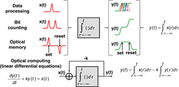
計算や情報処理向けの全光回路は、電子機器に固有の速度限界を破る可能性がある。しかし、フォトニクスでは、多機能電子回路に使われるものに対応する基本 的な「構成要素」はほとんど存在しない。本論文では、モノリシックな集積プラットフォームにおける最初の全光時間積分器を報告する。我々のデバイスは、受 動型マイクロリング共振器を利用した光波の「キャパシタに似た」素子であり、数ピコ秒の分解能で、任意の光波形の複雑な場の時間積分を行う。この分解能 は、約200 GHzの処理速度と1ナノ秒に近い「保持」時間に相当する。このデバイスは、電子技術(相補型金属酸化膜半導体)と互換性があり、次世代超高速データ処理 技術の構成要素の1つとなって、光メモリーやリアルタイムで微分方程式を計算する装置が可能になるであろう。
- INRS-EMT(カナダ)
All-optical circuits for computing and information processing could overcome the speed limitations intrinsic to electronics. However, in photonics, very few fundamental 'building blocks' equivalent to those used in multi-functional electronic circuits exist. In this study, we report the first all-optical temporal integrator in a monolithic, integrated platform. Our device—a lightwave 'capacitor-like' element based on a passive micro-ring resonator—performs the time integral of the complex field of an arbitrary optical waveform with a time resolution of a few picoseconds, corresponding to a processing speed of ∼200 GHz, and a 'hold' time approaching a nanosecond. This device, compatible with electronic technology (complementary metal-oxide semiconductor), will be one of the building blocks of next-generation ultrafast data-processing technology, enabling optical memories and real-time differential equation computing units.