Research Abstract
低電圧ウエアラブルセンサー応用を目指した非常に薄い印刷型有機TFT・CMOS論理回路の作製
Fabrication of Ultra-Thin Printed Organic TFT CMOS Logic Circuits Optimized for Low-Voltage Wearable Sensor Applications
2016年5月9日 Scientific Reports 6 : 25714 doi: 10.1038/srep25714
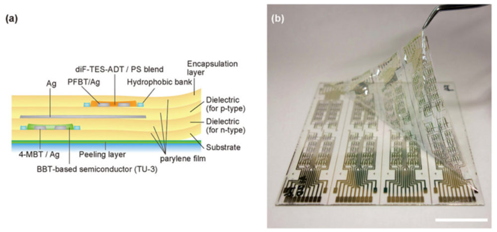
印刷技術を用いて製造できる超薄型電子回路は、ウエアラブル健康センサーや次世代フレキシブル電子デバイスの実現に重要となるデバイスである。p型とn型の半導体を組み合わせた相補型(CMOS)回路は、消費電力が少ないため、ワイヤレスデバイスなどに容易に利用することができる。今回我々は、ソース/ドレイン電極だけでなく半導体層も印刷技術で作製した超薄型CMOS論理回路について報告する。Dフリップフロップ回路には、新たに開発したp型とn型の有機薄膜トランジスタを用いた積層構造CMOS回路を用いた。これらのトランジスタは、p型で0.34 cm2 V−1 sec−1、n型で0.21 cm2 V−1 sec−1という良好な移動度を低電圧動作で実現するとともに、ほぼ0 Vのしきい値電圧など、優れた電気的特性を示した。この印刷型有機CMOS・Dフリップフロップ回路は75 Hzの動作周波数を示したことから、特にワイヤレス接続のウエアラブルセンサーなどのフレキシブル・プリンテッド・エレクトロニクス用として大きな可能性を実証するものである。
Corresponding Author
Ultrathin electronic circuits that can be manufactured by using conventional printing technologies are key elements necessary to realize wearable health sensors and next-generation flexible electronic devices. Due to their low level of power consumption, complementary (CMOS) circuits using both types of semiconductors can be easily employed in wireless devices. Here, we describe ultrathin CMOS logic circuits, for which not only the source/drain electrodes but also the semiconductor layers were printed. Both p-type and n-type organic thin film transistor devices were employed in a D-flip flop circuit in the newly developed stacked structure and exhibited excellent electrical characteristics, including good carrier mobilities of 0.34 and 0.21 cm2V−1sec−1, and threshold voltages of nearly 0 V with low operating voltages. These printed organic CMOS D-flip flop circuits exhibit operating frequencies of 75 Hz and demonstrate great potential for flexible and printed electronics technology, particularly for wearable sensor applications with wireless connectivity.