Research Abstract
非接触マイクロ波技術を用いた絶縁体–半導体界面における本質的な電荷キャリア輸送の評価
Evaluation of Intrinsic Charge Carrier Transport at Insulator-Semiconductor Interfaces Probed by a Non-Contact Microwave-Based Technique
2013年11月11日 Scientific Reports 3 : 3182 doi: 10.1038/srep03182
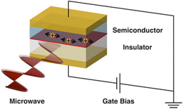
我々は、マイクロ波空洞共振器と薄い金属電極の形状を設計し、金属–絶縁体–半導体(MIS)素子構造を導入したマイクロ波空洞共振器を共振させることに成功した。この非常に単純なMIS素子は空洞共振器内で動作し、そこでは印加電圧によって絶縁体–半導体界面に電荷キャリアが定量的に注入される。同時に、導入されたマイクロ波によって、電荷キャリアの局所運動が直接検出され、注入電荷キャリア密度に対する定量的応答と充放電特性も同時に観測された。電場誘起時間分解マイクロ波伝導度法(FI-TRMC)と名付けられたこの測定システムを利用することにより、MIS素子中のペンタセン薄膜について、絶縁体–半導体界面のホール移動度を6.3 cm2 V−1 s−1、電子移動度を0.34 cm2 V−1 s−1と見積もることができた。本論文では、界面における本質的な電荷キャリア移動度を初めて直接・非接触的に測定し、実験的に十分検証されたその測定結果について報告する。
本庄 義人1, 宮階 智代1, 櫻井 庸明1, 佐伯 昭紀1 & 関 修平1
- 大阪大学工学研究科応用化学専攻
We have successfully designed the geometry of the microwave cavity and the thin metal electrode, achieving resonance of the microwave cavity with the metal-insulator-semiconductor (MIS) device structure. This very simple MIS device operates in the cavity, where charge carriers are injected quantitatively by an applied bias at the insulator-semiconductor interface. The local motion of the charge carriers was clearly probed through the applied external microwave field, also giving the quantitative responses to the injected charge carrier density and charge/discharge characteristics. By means of the present measurement system named field-induced time-resolved microwave conductivity (FI-TRMC), the pentacene thin film in the MIS device allowed the evaluation of the hole and electron mobility at the insulator-semiconductor interface of 6.3 and 0.34 cm2 V−1 s−1, respectively. This is the first report on the direct, intrinsic, non-contact measurement of charge carrier mobility at interfaces that has been fully experimentally verified.