Research Abstract
光でデザインするテラヘルツデバイス
Photo-designed terahertz devices
2011年10月18日 Scientific Reports 1 : 121 doi: 10.1038/srep00121
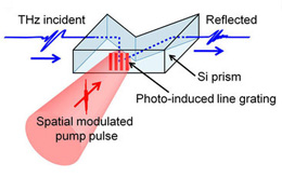
基本的な光デバイスを作製するため、フォトニック結晶やメタマテリアルなどの人工構造材料を用いた電磁波の操作技術が開発されつつある。例えば、金属周期構造体は、テラヘルツ周波数領域で動作するデバイスとして有望である。今回我々は、光でデザインするテラヘルツデバイスを実現し、リアルタイムかつ広帯域なテラヘルツ電磁波の周波数変調を可能にした。このデバイスは、平面状の光誘起周期導体構造であり、空間変調されたフェムト秒パルスレーザーをシリコン表面に照射することで形成される。変調周波数は構造の周期性によって調整できるが、光ポンプパルスのパワーにはほとんど影響を受けない。我々は、今回の発見が光集積回路などの光だけで操作する小型デバイス実現への道を開き、さらに、材料の製造工程を省くことが可能であると考えている。
- 京都大学 学際融合教育研究推進センター次世代開拓研究ユニット
- 京都大学 物質–細胞統合システム拠点
Technologies are being developed to manipulate electromagnetic waves using artificially structured materials such as photonic crystals and metamaterials, with the goal of creating primary optical devices. For example, artificial metallic periodic structures show potential for the construction of devices operating in the terahertz frequency regime. Here we demonstrate the fabrication of photo-designed terahertz devices that enable the real-time, wide-range frequency modulation of terahertz electromagnetic waves. These devices are comprised of a photo-induced, planar periodic-conductive structure formed by the irradiation of a silicon surface using a spatially modulated, femtosecond optical pulsed laser. We also show that the modulation frequency can be tuned by the structural periodicity, but is hardly affected by the excitation power of the optical pump pulse. We expect that our findings will pave the way for the construction of all-optical compact operating devices, such as optical integrated circuits, thereby eliminating the need for materials fabrication processes.