Research Abstract
STEM-EELSによるヘキサクロロフタロシアニン銅有機分子結晶の結晶欠陥の直接観察
Direct observation of crystal defects in an organic molecular crystals of copper hexachlorophthalocyanine by STEM-EELS
2012年2月7日 Scientific Reports 2 : 252 doi: 10.1038/srep00252
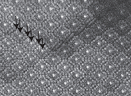
有機薄膜中の結晶欠陥の構造解析を行うことによって、電界効果トランジスターなどの用途向けの電子的特性に関する基本的知見が得られる。これまで、有機薄膜中の結晶欠陥の観察は、位相差イメージングに基づく従来型の透過電子顕微鏡法で行われてきたが、分解能はかなり低かった。今回我々は、収差補正走査型透過電子顕微鏡と電子エネルギー損失分光を併用することによってヘキサクロロフタロシアニン銅薄膜中の粒界を原子分解能レベルで直接観察するために、円環暗視野イメージングを初めて適用している。我々は、低線量技術の利用と検出角の最適化によって、分子カラム内の重い元素(Cl、Cu)とともに軽元素(C、N)のコントラストも可視化できた。また、{110}結晶面に沿った結晶粒界において積層欠陥をもたらす予想外の分子配列を確認できた。
- 京都大学化学研究所
The structural analysis of crystal defects in organic thin films provides fundamental insights into their electronic properties for applications such as field effect transistors. Observation of crystal defects in organic thin films has previously been performed at rather low resolution by conventional transmission electron microscopy based on phase-contrast imaging. Herein, we apply for the first time annular dark-field imaging to the direct observation of grain boundaries in copper hexachlorophthalocyanine thin films at the atomic resolution level by using an aberration-corrected scanning transmission electron microscope combined with electron energy-loss spectroscopy. By using a low-dose technique and an optimized detection angle, we were able to visualize the contrast of light element (C and N) together with the heavier elements (Cl and Cu) within the molecular column. We were also able to identify unexpected molecular orientations in the grain boundaries along the {110} crystallographic planes giving rise to stacking faults.