デバイス用液晶の配向およびスイッチングを目的とした、高解像度表面ナノパターンを持つ二機能性ITO
Bifunctional ITO layer with a high resolution, surface nano-pattern for alignment and switching of LCs in device applications.
2012年2月17日 NPG Asia Materials 4, e2 (2012) doi:10.1038/am.2012.12
表面パターニング:液晶を制御する
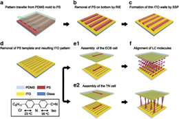
Hee-Tae JungおよびShin-Woong Kangの研究チームが、効率的な液晶デバイスの作製方法を考案した。液晶デバイスは、2つの電極に挟まれた液晶(液体のように流れるが、結晶のように広範囲にわたって配向する分子)層から構成される。液晶配向の制御によって光の調節(調光)は可能だが、そのためには通常、追加的な構成要素や加工過程が必要となる。研究チームはこのたび、イオン衝撃と鋳型材を利用したリソグラフィー技術で、導電性インジウムスズ酸化物(ITO)膜にストライプパターンを形成した。この方法でパターニングされたITOは2つの機能を持ち、電極としての役割と、大面積にわたって液晶配向を制御する手段(配向膜)としての役割を果たす。パターニング後のITOを用いて作製したデバイスは、良好な電気光学特性を示しており、この技術の実用化が期待される。
Surface patterning: Liquid crystals under control
Hee-Tae Jung, Shin-Woong Kang and co-workers have devised an efficient way to prepare liquid-crystal devices. These devices comprise a layer of liquid crystals – molecules that flow as in a liquid state yet can be aligned over large areas in a crystalline manner – sandwiched between two electrodes. Controlling the orientation of the liquid crystals can be used to modulate light, but this is usually achieved through additional components or processing steps. Relying on a lithographic technique, the researchers have now used ion bombardment and a mould material to create stripes on the surface of an electrically conductive indium tin oxide surface. The resulting material is bifunctional, serving as both an electrode and a way to control the alignment of the liquid crystals over large domains. Devices constructed using indium tin oxide patterned in this way have shown good electro-optical properties, making this technique promising for practical applications.