単原子の電場イメージング
Electric field imaging of single atoms
2017年5月30日 Nature Communications 8 : 15631 doi: 10.1038/ncomms15631
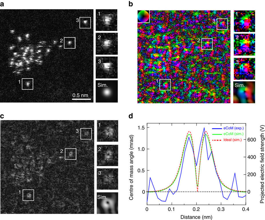
走査型透過電子顕微鏡(STEM)では、高角度に散乱された電子を試料下方にある環状検出器を用いて検出することにより、単原子を可視化できる。最近、原子分解能の微分位相コントラストSTEMによって、結晶物質を構成する原子カラム内部の原子核とその周囲にある電子の間に存在する電場を直接プローブできることが示されている。今回我々は、多分割型検出器を組み込んだサブオングストローム空間分解能を有するSTEMを用いて、単一金原子内部の(投影された)原子電場分布の実空間画像化に成功した。我々は、単一金原子内部の電場分布(注:真の電場分布が電子プローブによってぼかされたもの)が、原子内部の全電荷密度の空間変動に連動して大きく変化する様子を直接可視化することに成功した。単原子レベルの感度を有する原子分解能の電場マッピングによって、原子の内部構造やその境界構造を詳しく調べることが可能になると期待できる。
Corresponding Author
In scanning transmission electron microscopy (STEM), single atoms can be imaged by detecting electrons scattered through high angles using post-specimen, annular-type detectors. Recently, it has been shown that the atomic-scale electric field of both the positive atomic nuclei and the surrounding negative electrons within crystalline materials can be probed by atomic-resolution differential phase contrast STEM. Here we demonstrate the real-space imaging of the (projected) atomic electric field distribution inside single Au atoms, using sub-Å spatial resolution STEM combined with a high-speed segmented detector. We directly visualize that the electric field distribution (blurred by the sub-Å size electron probe) drastically changes within the single Au atom in a shape that relates to the spatial variation of total charge density within the atom. Atomic-resolution electric field mapping with single-atom sensitivity enables us to examine their detailed internal and boundary structures.