双極子禁制則を破ることによるSnO2系紫外発光ダイオードの実現
Realizing a SnO2-based ultraviolet light-emitting diode via breaking the dipole-forbidden rule
2012年11月9日 NPG Asia Materials 4, e11 (2012) doi:10.1038/am.2012.56
光学材料:禁制ギャップを克服
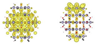
酸化物半導体の電子構造には一般的に、伝導帯と価電子帯の間に広いエネルギーギャップがある。そのため、酸化物半導体は高効率紫外発光体になると考えられ、照明、ディスプレイ、フォトニックデバイスの構成要素として期待されている。ところが多くの場合、こうした発光をもたらす電子状態間の光学遷移は、量子力学では禁止されている。Tom WuおよびSu-Huai Wei率いる研究チームはこのたび、二酸化スズのナノスケール構造、特にその有効表面を変化させることによって、この問題を回避することに成功した。彼らはまず計算を行い、その結果をもとにアニール処理を経てナノ結晶-アモルファスハイブリッド薄膜を作製、さらに、その二酸化スズ薄膜を用いて高効率UV発光ダイオードを作製した。これらの研究結果は、ナノ構造設計によってほかの酸化物も光学活性化できる可能性があることを示唆している。
Optical materials: Over the forbidden gap
Oxide semiconductors typically possess wide energy gaps between the conduction and valence bands in their electronic structure. This predisposes them to be efficient ultraviolet light emitters, and thus promising components in lighting, display and photonic devices. Yet, in most cases, the optical transition between electronic states that is responsible for this emission is a forbidden one in quantum mechanics. A research team led by Tom Wu and Su-Huai Wei has now circumvented this issue with tin dioxide by altering the material's nanoscale structure, in particular its effective surface. Calculations were carried out that subsequently guided the preparation of hybrid nanocrystalline-amorphous thin films through an annealing step. The tin dioxide thin films were then used to construct an efficient UV light-emitting diode. These findings suggest that engineering the nanostructure of other oxides might also render them optically active.