柔軟性と伸縮性のある生体融和型エレクトロニクス向けの無機半導体ナノ材料
Inorganic semiconductor nanomaterials for flexible and stretchable bio-integrated electronics.
2012年4月20日 NPG Asia Materials 4, e4 (2012) doi:10.1038/am.2012.27
半導体:曲げたり伸ばしたり
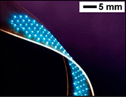
半導体は、条件に応じて導電体か絶縁体のいずれかの機能を果たす材料であり、従来は無機半導体が多く使われてきた。エレクトロニクスの基礎を成すこうした半導体は、多くのデバイスで極めて重要な役割を果たしている。John Rogersをはじめとする研究チームはこのたび、無機半導体ナノワイヤーやナノ膜の作製、無機半導体と有機部品とを組み合わせたハイブリッド材料の作製、さらにそれらの材料のデバイスへの組み込みなどを可能にした最近の進展について論じている。無機半導体ナノ材料の一次元構造体や二次元構造体を利用することにより、柔軟性と伸縮性を持つエレクトロニクスデバイスやオプトエレクトロニクスデバイスの作製が可能になる。柔軟性と伸縮性は多くの分野に応用が可能な特性であり、特に生体応用では有望だ。実際、これまでに、心臓や脳の電気的活動をマッピングできるシステムの構築や、ヒトの皮膚の特徴をまねた部品を用いた表皮電子デバイスの作製が行われたりしている。こうしたデバイスは、機能的活動のモニタリングや治療的介入に有望である。
Semiconductors: Bending and stretching
Semiconductors are materials — traditionally inorganic ones — that can act as either conductors or insulators under different conditions. They form the foundation of electronics and play a crucial role in many devices. John Rogers and co-workers discuss recent advances that have made possible the preparation of inorganic semiconductors as nanowires or nanomembranes, their assembly together with organic components into hybrid materials, and their integration into devices. These one- and two-dimensional structures allow for the construction of electronic or opto-electronic devices that are flexible and stretchable — properties that are particularly, albeit not exclusively, promising for biological applications. Systems capable of mapping the electrical activity of the heart and brain have been built, and assemblies whose characteristics mimic those of human skin have led to the construction of epidermal electronic devices. Such devices hold promise for monitoring functional activity and for therapeutic interventions.