Research Abstract
サブミクロン精細度の導電性銀パターン形成のためのナノ粒子化学吸着印刷技術
Nanoparticle chemisorption printing technique for conductive silver patterning with submicron resolution
2016年4月19日 Nature Communications 7 : 11402 doi: 10.1038/ncomms11402
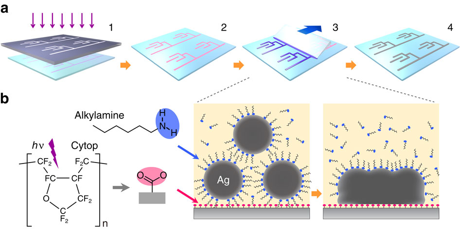
銀ナノコロイド(配位子で被覆された銀ナノ粒子の濃厚懸濁液)は、印刷を用いたデバイス製造技術に向けた有力な材料である。しかし、従来の印刷技術の効用はきわめて限定的であるため、工業製品化向けの十分に高い品質と精細度を有する導電性印刷パターンはいまだ得られていない。今回我々は、弱く被覆された銀ナノ粒子が、光で活性化された表面上にのみ限られて化学吸着する現象を利用して、超高精細な導電性パターンを製造する印刷技術を開発したので報告する。このプロセスでは、非晶質パーフルオロポリマー層にマスクを通して真空紫外光を照射しカルボキシル基を配した光活性表面を形成した後、アルキルアミンで被覆した銀ナノコロイドでこの表面をコーティングすると、アミン-カルボキシル基変換が起こり、自己融着した固体銀層が自発的に形成される。この手法により、基材に強く密着したサブミクロン精細度の銀パターンが得られ、結果としてフレキシブルな透明導電性シートの製造が可能になる。今回の印刷法は、真空やフォトリソグラフィーを利用した従来のデバイス加工法に取って代わる可能性がある。
Corresponding Authors
Silver nanocolloid, a dense suspension of ligand-encapsulated silver nanoparticles, is an important material for printing-based device production technologies. However, printed conductive patterns of sufficiently high quality and resolution for industrial products have not yet been achieved, as the use of conventional printing techniques is severely limiting. Here we report a printing technique to manufacture ultrafine conductive patterns utilizing the exclusive chemisorption phenomenon of weakly encapsulated silver nanoparticles on a photoactivated surface. The process includes masked irradiation of vacuum ultraviolet light on an amorphous perfluorinated polymer layer to photoactivate the surface with pendant carboxylate groups, and subsequent coating of alkylamine-encapsulated silver nanocolloids, which causes amine–carboxylate conversion to trigger the spontaneous formation of a self-fused solid silver layer. The technique can produce silver patterns of submicron fineness adhered strongly to substrates, thus enabling manufacture of flexible transparent conductive sheets. This printing technique could replace conventional vacuum- and photolithography-based device processing.