Research Abstract
ポリマー薄膜トランジスタの簡易プッシュコーティング
Simple push coating of polymer thin-film transistors
2012年11月6日 Nature Communications 3 : 1176 doi: 10.1038/ncomms2190
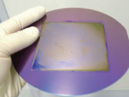
溶液プロセスによる加工性は有機半導体に固有な特長であり、これにより大気下においてフレキシブルな電子装置を安価に生産することが可能になる。しかしながら、基板表面の溶液との親しみやすさは、なお深刻なジレンマである。すなわち、撥水性の高い表面では液体の操作がより難しくなるが、このような表面の利用はデバイスの特性を改善するうえで不可欠なのである。今回我々は、材料の無駄をなくしつつ、撥水性表面に均一で大面積のポリマー半導体薄膜を製造するための、簡易な「プッシュコーティング」と呼ぶ技術について実証を行う。我々はポリジメチルシロキサンを用いた3層構造のスタンプを用いている。このスタンプは、基板と等形接触し、毛管現象によって表面を濡らすことができる。スタンプが溶媒を吸収し保持することによって薄膜が形成され、かつこれにより、スタンプを薄膜から完全に剝がすことができる。撥水性の高い表面に平らな薄膜が形成されるので、製膜後に薄膜の微細パターンニングを施すことも可能である。この手法によりスタンプによって作製した半導体薄膜の結晶性と電界効果移動度を向上できることは、フレキシブルな電子装置の生産に向けた大きな一歩となる。
井川 光弘1, 山田 寿一1, 松井 弘之1, 峯廻 洋美1, 堤 潤也1, 堀井 美徳1, 近松 真之1, 阿澄 玲子1, 熊井 玲児2 & 長谷川 達生 1
- 独立行政法人 産業技術総合研究所(AIST)
- 放射光科学研究施設(PF)および構造物性研究センター(CMRC)物質構造科学研究所高エネルギー加速器研究機構(KEK)
Solution processibility is a unique advantage of organic semiconductors, permitting the low-cost production of flexible electronics under ambient conditions. However, the solution affinity to substrate surfaces remains a serious dilemma; liquid manipulation is more difficult on highly hydrophobic surfaces, but the use of such surfaces is indispensable for improving device characteristics. Here we demonstrate a simple technique, which we call ‘push coating’, to produce uniform large-area semiconducting polymer films over a hydrophobic surface with eliminating material loss. We utilize a poly(dimethylsiloxane)-based trilayer stamp whose conformal contact with the substrate enables capillarity-induced wetting of the surface. Films are formed through solvent sorption and retention in the stamp, allowing the stamp to be peeled perfectly from the film. The planar film formation on hydrophobic surfaces also enables subsequent fine film patterning. The technique improves the crystallinity and field-effect mobility of stamped semiconductor films, constituting a major step towards flexible electronics production.