Research Abstract
シリコン中の逆スピンホール効果の観測
Observation of the inverse spin Hall effect in silicon
2012年1月17日 Nature Communications 3 : 629 doi: 10.1038/ncomms1640
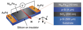
固体におけるスピン軌道相互作用は、電子のスピンと運動量を結合する。この結合によって、スピン流と電流の相互変換、つまりスピンホール効果と逆スピンホール効果が生じる。スピンホール効果は、金属や半導体で観測されている。しかし、スピン流-電流変換は最も重要な半導体であるシリコンでは実現されておらず、シリコンのスピン軌道相互作用が極めて弱いため、スピンホール効果の利用は難しいと考えられている。今回我々は、室温におけるシリコン中の逆スピンホール効果の観測について報告する。その結果、p型シリコン薄膜で0.0001のスピン流-電流変換効率、つまりスピンホール角が得られている。スピンホール角は小さいが、p型シリコン薄膜において逆スピンホール効果に起因する明瞭な電圧が確認されており、シリコンをスピン流検出器として利用できることが実証されている。
- 東北大学 金属材料研究所
- 科学技術振興機構(JST)戦略的創造研究推進事業(CREST)
- 日本原子力研究開発機構 先端基礎研究センター
The spin–orbit interaction in a solid couples the spin of an electron to its momentum. This coupling gives rise to mutual conversion between spin and charge currents: the direct and inverse spin Hall effects. The spin Hall effects have been observed in metals and semiconductors. However, the spin/charge conversion has not been realized in one of the most fundamental semiconductors, silicon, where accessing the spin Hall effects has been believed to be difficult because of its very weak spin–orbit interaction. Here we report observation of the inverse spin Hall effect in silicon at room temperature. The spin/charge current conversion efficiency, the spin Hall angle, is obtained as 0.0001 for a p-type silicon film. In spite of the small spin Hall angle, we found a clear electric voltage due to the inverse spin Hall effect in the p-Si film, demonstrating that silicon can be used as a spin-current detector.