Research Abstract
カーボンナノチューブ接合部内におけるジュール加熱ダイナミクスおよび温度プロファイリングの直接画像化
カーボンナノチューブなどの基本的なナノ電子デバイス構成材における抵抗(ジュール)加熱を理解すること、特に長時間の電気的ストレス時の構造的・熱的変化に関して理解することは、依然として大きな課題である。
Direct imaging of Joule heating dynamics and temperature profiling inside a nanotube interconnect
2011年8月9日 Nature Communications 2 : 421 doi: 10.1038/ncomms1429
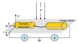
カーボンナノチューブなどの基本的なナノ電子デバイス構成材における抵抗(ジュール)加熱を理解すること、特に長時間の電気的ストレス時の構造的・熱的変化に関して理解することは、依然として大きな課題である。今回我々は、カーボンナノチューブ接合チャネルにおけるジュール加熱関連の影響をリアルタイムで画像化したことを示す。最初に、透過電子顕微鏡内において、昇華性物質で完全に満たしたナノチューブとの電気接点を形成している。高密度電流を流すと、接点上(または付近)に抵抗性ホットスポットが確認される。封入物質の局所的昇華から明らかなように、これらのホットスポットは、その後、カーボンナノチューブに沿って移動・拡大する。このホットスポット端をマーカーとして用いることにより、ナノチューブの内部温度プロファイルを推定できる。単純かつ直接的な我々の方法によって、抵抗性ホットスポットのダイナミクスやナノスケールのチューブ接合部内で起こるミリ秒ペースの熱的変化に関して、注目すべき空間的・時間的知見が得られる。
- アヴェイロ大学(ポルトガル)
- ドレスデン・ライプニッツ固体・加工材料研究所(ドイツ)
-
独立行政法人 物質・材料研究機構 国際ナノアーキテクトニクス研究拠点
*(現所属)ネルー先端科学研究所(インド)
Understanding resistive (or Joule) heating in fundamental nanoelectronic blocks, such as carbon nanotubes, remains a major challenge, particularly in regard to their structural and thermal variations during prolonged periods of electrical stress. Here we show real-time imaging of the associated effects of Joule heating in the channel of carbon nanotube interconnects. First, electrical contacts to nanotubes entirely filled with a sublimable material are made inside a transmission electron microscope. On exposure to a high current density, resistive hotspots are identified on (or near) the contact points. These later migrate and expand along the carbon nanotube, as indicated by the localized sublimation of the encapsulated material. Using the hotspot edges as markers, it is possible to estimate the internal temperature profiles of the nanotube. Simple and direct, our method provides remarkable spatial and temporal insights into the dynamics of resistive hotspots and millisecond-paced thermal variations occurring inside nanoscaled tubular interconnects.