Research Abstract
半導体表面上の金属的表面状態バンドにおける大きなRashbaスピン分裂
スピン偏極した電子を室温で作ることは、半導体スピントロニクスの開発に不可欠な一歩である。
Large Rashba spin splitting of a metallic surface-state band on a semiconductor surface
2010年5月17日 Nature Communications 1 : 17 doi: 10.1038/ncomms1016
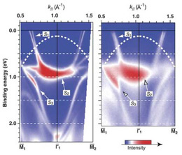
スピン偏極した電子を室温で作ることは、半導体スピントロニクスの開発に不可欠な一歩である。我々は、この目的のために、被覆率4/3の鉛単原子層に覆わ れたGe(111)表面の電子状態を、角度分解光電子分光(ARPES)、スピン分解ARPES、第一原理電子状態計算で調べた。Pb 6p の性質を有する金属的表面状態バンドが、フェルミ準位において200 meVの大きなRashbaスピン分裂と有効質量0.028 meを示すことが実証された。この発見によって、半導体表面におけるスピン輸送/蓄積という新たな分野の材料基盤が得られる。表面状態の電荷密度解析により、大きなスピン分裂はPb原子の原子核近傍の電荷密度が非対称であることに由来していることがわかった。
- 京都大学大学院理学研究科化学専攻
- JST-CREST
- 広島大学放射光科学研究センター
- 広島大学大学院理学研究科
The generation of spin-polarized electrons at room temperature is an essential step in developing semiconductor spintronic applications. To this end, we studied the electronic states of a Ge(111) surface, covered with a lead monolayer at a fractional coverage of 4/3, by angle-resolved photoelectron spectroscopy (ARPES), spin-resolved ARPES and first-principles electronic structure calculation. We demonstrate that a metallic surface-state band with a dominant Pb 6p character exhibits a large Rashba spin splitting of 200 meV and an effective mass of 0.028 me at the Fermi level. This finding provides a material basis for the novel field of spin transport / accumulation on semiconductor surfaces. Charge density analysis of the surface state indicated that large spin splitting was induced by asymmetric charge distribution in close proximity to the nuclei of Pb atoms.