The Missing Kingdom: Why Fungi Must Be Central to Conservation Strategy
28 December 2025
Published online 9 September 2022
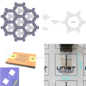
A new 2D polycrystalline material incorporates fast electrical conductivity with a band gap, promising new optoelectronic devices.
Hyuk-Jun Noh 2022
The development comes from a research team in South Korea working with materials scientist Javeed Mahmood, at King Abdullah University of Science and Technology (KAUST), in Saudi Arabia.
This innovation is part of the growing effort to develop and exploit 2D materials that consist of atom-thick layers, or a few such layers, extending relatively widely across two dimensions.
“Devices using [our material] as active layers show remarkable performances, indicating vast potential for applications in thin-film optoelectronic devices,” says Mahmood. Optoelectronics interconvert optical and electrical signals in applications such as sensors, communications devices and novel forms of computing.
The push to explore new 2D materials stems from limitations in the electrical properties of graphene, the best-known such structure, which is composed of many linked rings of six carbon atoms. Graphene exhibits limitations in electrical conduction and the ability to control the conduction, making it unsuitable for most optoelectronic and semi-conductor applications.
The new ‘fused aromatic network’ (FAN) material incorporates nitrogen atoms within many of its six-atom rings, with these rings connected into larger rings, which are themselves all interconnected across a wide flat molecular array. This structure permits fast electron transport – the essential feature of an electric current – but crucially also incorporates a suitable and vital aspect of semi-conductor materials called a band gap. This means that a specific amount of energy is needed to kick electrons into their conducting state, allowing the fine control and switching on and off of the essential current for microelectronic and optoelectronic applications.
Ali Coskun, a chemist at the University of Fribourg in Switzerland, who was not involved in the research, comments: "This work represents a significant step forward towards understanding the charge transport behaviour in two-dimensional porous organic semiconductors and will certainly open new applications. However, it is still a daunting challenge to synthesize large-area and defect-free films of these materials."
Mahmood says the team plans to address that challenge with the ultimate aim of making single crystals large enough for any working device.
doi:10.1038/nmiddleeast.2022.51
Hyuk-Jun Noh et al. Hydrophenazine-linked two-dimensional ladder-type crystalline fused aromatic network with high charge transport. Chem 8, 1-15 (2022).
28 December 2025
24 December 2025
24 December 2025
01 June 2022
22 March 2021
29 September 2020
Sign-up to receive our e-alert update every two weeks to keep up with everything new on the portal.
Sign up for e-alerts
Stay connected: