Research Abstract
金属/有機半導体実界面における電荷注入機構の解明
On Practical Charge Injection at the Metal/Organic Semiconductor Interface
2013年1月4日 Scientific Reports 3 : 1026 doi: 10.1038/srep01026
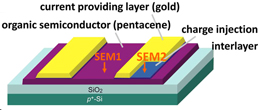
二層電極構造を有する有機トランジスタ構造を用いて、金属/有機半導体実界面における電荷注入機構を評価することに成功した。電極と有機半導体の間に膜厚数ナノメートルの金属を界面金属層として挿入することにより、界面金属のみが注入機構へ与える依存性を解明できるようになった。一般的に金属/有機半導体界面における電荷注入機構において、最も考慮すべき点は、仕事関数の大きい金属を用いて有機半導体のエネルギー準位の間に生じる障壁を小さくできるかが重要であると考えられている。しかし、素子構造作製時に大気曝露される実界面では、従来の仕事関数の大きい界面金属を用いても電荷注入が改善せず、またそれらの相関関係は得られなかった。そこで、金属の酸化還元反応の指標である標準電極電位と電荷注入を比較したところ、酸化還元電位に大きく依存し、電荷注入が飛躍的に改善することが明瞭になった。これは、酸化還元電位が接触界面での電荷注入機構に最も支配的な影響を及ぼすことを示唆している。この機構の解明は、さまざまな有機半導体実デバイスに応用可能であり、実効的な電荷注入の制御するための進展である。
熊谷 明哉1*, Yun Li1†, Peter Darmawan1, 三成 剛生1 & 塚越 一仁1, 2
- 独立行政法人 物質・材料研究機構 国際ナノアーキテクトニクス研究拠点(WPI-MANA)
- 独立行政法人 科学技術振興機構 戦略的創造研究推進事業(JST-CREST)
*現所属: 東北大学 原子分子材料科学高等研究機構(WPI-AIMR)
†現所属: 南京大学 光・電子材料研究所および電子科学与工程学院(中国)
We have revealed practical charge injection at metal and organic semiconductor interface in organic field effect transistor configurations. We have developed a facile interface structure that consisted of double-layer electrodes in order to investigate the efficiency through contact metal dependence. The metal interlayer with few nanometers thickness between electrode and organic semiconductor drastically reduces the contact resistance at the interface. The improvement has clearly obtained when the interlayer is a metal with lower standard electrode potential of contact metals than large work function of the contact metals. The electrode potential also implies that the most dominant effect on the mechanism at the contact interface is induced by charge transfer. This mechanism represents a step forward towards understanding the fundamental physics of intrinsic charge injection in all organic devices.