Research Abstract
シリコンチップ上にモノリシックに集積された偏光量子もつれ光子対源
A monolithically integrated polarization entangled photon pair source on a silicon chip
2012年11月12日 Scientific Reports 2 : 817 doi: 10.1038/srep00817
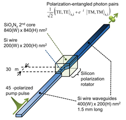
集積光回路は、小さな素子サイズや、安定かつ空間モード重なりがほぼ完全な経路干渉計を有するため、大規模光量子情報処理システムの最も有望なプラットフォームの1つである。とりわけ多くの量子情報プロトコルにおいて、光子の偏光に基づく量子ビットが用いられているため、集積チップ上で偏光に関する量子状態を生成、操作、測定する素子の開発が必要である。特にその生成素子は重要だ。今回我々は、初めてチップ上に集積された偏光量子もつれ光子対源を示す。我々は、簡便かつ安定な構成のSOI(Silicon on Insulator)光回路としてこの光源を実装し、偏光量子もつれ状態を91±2%の忠実度で生成することに成功した。本光源は、石英系導波路をはじめとする種々の導波路プラットフォームへの接続を可能とするインターフェースを備えており、偏光に関する操作・射影素子やポンプ光源の一体化集積が可能である。したがって、チップ上に光量子情報処理システムを完全集積する準備ができた。
松田 信幸1, 3, Hanna Le Jeannic1*, 福田 浩2, 3, 土澤 泰2, 3, William John Munro1, 清水 薫1, 山田 浩治2, 3, 都倉 康弘1† & 武居 弘樹1
- NTT物性科学基礎研究所
- NTTマイクロシステムインテグレーション研究所
- NTTナノフォトニクスセンタ
*現所属:パリ市立工業物理化学大学院大学
†現所属:筑波大学大学院 数理物質科学研究科
Integrated photonic circuits are one of the most promising platforms for large-scale photonic quantum information systems due to their small physical size and stable interferometers with near-perfect lateral-mode overlaps. Since many quantum information protocols are based on qubits defined by the polarization of photons, we must develop integrated building blocks to generate, manipulate, and measure the polarization-encoded quantum state on a chip. The generation unit is particularly important. Here we show the first integrated polarization-entangled photon pair source on a chip. We have implemented the source as a simple and stable silicon-on-insulator photonic circuit that generates an entangled state with 91 ± 2% fidelity. The source is equipped with versatile interfaces for silica-on-silicon or other types of waveguide platforms that accommodate the polarization manipulation and projection devices as well as pump light sources. Therefore, we are ready for the full-scale implementation of photonic quantum information systems on a chip.