Research Abstract
化学気相合成法で成長させたグラフェンの輸送移動度が相対的に低くなる原因
Origin of the relatively low transport mobility of graphene grown through chemical vapor deposition
2012年3月27日 Scientific Reports 2 : 337 doi: 10.1038/srep00337
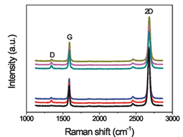
化学気相合成法で成長させたグラフェン(CVD-G)の輸送移動度が低くなる理由が、今回の研究で解明された。CVD-Gの伝導度を低下させる要因として、点欠陥、表面汚染物質、線欠陥が挙げられる。今回の研究は、CVD-Gの輸送移動度が低くなる決定的要因は、点欠陥や表面汚染によるのではなく、粒界によって引き起こされる欠陥に起因するものであることを明示している。まず、電子顕微鏡観察では、粒界の存在も明確となり、CVD-Gの多結晶性が示された。粒界のないCVD-Gを使った電界効果トランジスターの計測では、高品質剥離グラフェンに匹敵する輸送移動度が得られて、粒界に散乱要因が存在していることが明瞭となった。さらに、伝導の温度特性から、粒界を超える電気伝導はポテンシャル障壁モデルにて説明できる事が解った。本研究にて、CVD-Gの本質的な輸送特性の理解が可能となった。
- 独立行政法人物質・材料研究機構国際ナノアーキテクトニクス研究拠点
- 産業技術総合研究所 連携研究体グリーン・ナノエレクトロニクスセンター
The reasons for the relatively low transport mobility of graphene grown through chemical vapor deposition (CVD-G), which include point defect, surface contamination, and line defect, were analyzed in the current study. A series of control experiments demonstrated that the determinant factor for the low transport mobility of CVD-G did not arise from point defects or surface contaminations, but stemmed from line defects induced by grain boundaries. Electron microscopies characterized the presence of grain boundaries and indicated the polycrystalline nature of the CVD-G. Field-effect transistors based on CVD-G without the grain boundary obtained a transport mobility comparative to that of Kish graphene, which directly indicated the detrimental effect of grain boundaries. The effect of grain boundary on transport mobility was qualitatively explained using a potential barrier model. Furthermore, the conduction mechanism of CVD-G was also investigated using the temperature dependence measurements. This study can help understand the intrinsic transport features of CVD-G.